HD64180 Single Board Computer
Overview
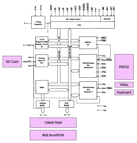
This is a SBC I am building using the Hitachi HD64B180 microprocessor. This is a block diagram of how I plan to compose the system:
Bare Minimum
Completed 7/7/26. Written 7/8/26.
Attach MPU to perfboard
This was done by spreading out the pins on the MPU (dead bug) and then hot gluing it to the top of the PCB
Clock circuit
The HD64180 has a built in oscillator. This made setting up the clock circuit both easier and harder.
It is easier because I don't have TTL oscillators that can be divided into standard baud rates and they can get a bit pricey. I do have 11.0592 MHz crystals which are divisible into common baud rates.
It is harder because I have to deal with load capacitors. I used 20µF load capacitors. I do not have the datasheet for the crystal so I picked capacitors that I already had available. The HD64180 is also only rated for 10 MHz. I tested with a oscilloscope and the crystal was oscillating at, from what I could tell, was the correct frequency and the address lines were pulsing correctly. Time will tell if overclocking the MPU by 1.0592 MHz (~10%) will be stable. It would be annoying to replace the crystal with a new one.
Pull-up resistors
The /WAIT, /BUSREQ, /NMI, /INT0, /INT1, and INT2 pins had to be pulled up. I don't expect to be needing to use these pins because this will be a simple SBC. But just to be safe I used pull-up resistors instead of pulling them directly to Vcc. The first two are pulled up with 1kΩ resistors. The rest are pulled up with 10kΩ resistors. I switched after doing the reset circuit because 10kΩ will use less power when the signal is driven low. Will it ever be driven low? Probably not.
Reset circuit
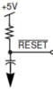
I used a button I desoldered off of a scrap alarm clock, a 10kΩ pull-up resistor, a 150nF debouncing capacitor, and no resistor between the /RESET pin and the reset circuit. This is the given reset circuit in the Z80 manual:
Power
I soldered two jumper wires that I will plug into an Arduino to grovide +5V and GND.
Mistakes and Issues
These mistakes were identified in the construction and fixed:
- Vcc was connected to GND. Thankfully, nothing happened because there is only one Vcc pin on the MPU.
- The last four pull-ups were tied to GND instead of Vcc by connecting them to the GND on the reset circuit instead of wiring them to Vcc.
- The reset pull-up resistor had not been connected to Vcc.
Photos
These are photographs of the front and back of the PCB so far:
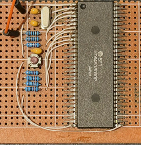
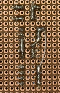
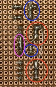
Colored circle meanings:
- Red: Vcc
- Blue: GND
- Magenta:
/RESET
RAM
I have a KM684000BLP 512kx8 SRAM IC that I will use as RAM. There will be no ROM. Instead, the OS (CP/M) will be stored in battery-backed RAM. This is dangerous because software can make the system unusable very easily by overwriting SRAM.
Upload Port
I will add an Arduino Mega compatible port that will give access to the SRAM.